When designing a circuit recently, I was faced with selecting appropriate load capacitors for the crystal oscillator on my microcontroller. While in the end this selection is rather straightforward, finding the relevant information can be a challenge. My Google searches weren't as helpful as I'd hoped they'd be, and I had to pull together information from several sources. I wrote this blog post to pull together all of the information I found into a single page that hopefully can serve as a reference for others.
So let's begin: what are load capacitors and why are they needed?
The oscillator used by most (all?) microcontrollers is known as a Pierce oscillator. To quote Wikipedia:
The Pierce oscillator is a type of electronic oscillator particularly well-suited for use in piezoelectric crystal oscillator circuits. Named for its inventor, George W. Pierce (1872-1956),[1][2] the Pierce oscillator is a derivative of the Colpitts oscillator. Virtually all digital IC clock oscillators are of Pierce type, as the circuit can be implemented using a minimum of components: a single digital inverter, two resistors, two capacitors, and the quartz crystal, which acts as a highly selective filter element. The low manufacturing cost of this circuit, and the outstanding frequency stability of the quartz crystal, give it an advantage over other designs in many consumer electronics applications.
In order to oscillate correctly, the oscillator needs a certain amount of capacitance across the leads of the crystal. This capacitance, known as the "load capacitance," forms an essential part of the oscillator circuit.
The required load capacitance is specified by the crystal manufacturer in the datasheet, usually as CL. The crystal manufacturer is saying that if the capacitance across the leads of the crystal is equal to CL, the crystal will resonate at its specified frequency.
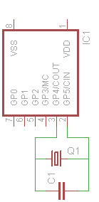
A naive solution to this problem is to simply use a single capacitor, of CL, across the leads of the crystal. Unfortunately, things aren't quite this easy. The naive solution looks like this:
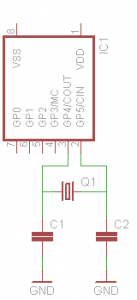
However, it's never done that way. Instead, load capacitors are placed from each lead of the crystal to ground. (I don't know why this is; I haven't yet found a good explanation in my research. If you have a good explanation, let us know in the comments!) The typical solution looks like this:
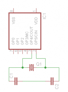
Note that electrically, this is equivalent to two capacitors in series, with the circuit's ground on the segment between the two load capacitors. We can redraw the above circuit like this:
Now we have a problem we can solve. If we want the capacitance across the leads of the cystal to be CL, and we have two capacitors in series, we can figure out what value C to use for the capacitors. The formula for capacitors in series is:
For two capacitors, this formula reduces to:
If we set C1 = C2 (which is almost always going to be the case with crystal load capacitors), and call that value C, we can further reduce this equation to:
So, it would appear that if we need to find C such that C/2 = CL, we should choose C = 2(CL), right?
Well... almost. If the load capacitors were the only capacitance across the leads of the crystal, that would indeed be the case. However, there are additional sources of capacitance in the oscillator circuit. The first source is the "stray capacitance" of the circuit board traces. The second is the input capacitance of the oscillator circuit on the microcontroller.
The input capacitance of the microcontroller's oscillator is specified in the datasheet. For the Atmel ATSAM3S controller I'm considering, it's specified in table 42-18 of the datasheet as 1pF typical.
The stray capacitance of the circuit board is a bit more difficult to come by. Apparently, this is a difficult measurement to make, so the usual approach is to just guess. I've seen anything from 2pF to 5pF given as an appropriate value, and 3-5pF seems to be the most common guess.
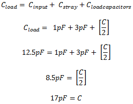
The crystal I've chosen for my circuit requires a load capacitance of 12.5pF to oscillate at its rated frequency. Choosing the load capacitors, then, looks like this:
For this circuit, then, I'm going to use 18pF capacitors for C1 and C2.
Crystal 'Pulling'
So what happens then if we choose the wrong value for the load capacitors?
Quoting Microchip App Note AN826 (linked below), crystals can be pulled from their specified operating frequency by adjusting the load capacitance the crystal sees in the circuit. An approximate equation for crystal pulling limits is:
Where:
Δf = the pulled crystal frequency minus fs
fs = the crystal's resonant frequency
C1 = the motional arm capacitance of the crystal
C0 = the shunt capacitance of the crystal
CL = the actual load capacitance across the crystal's leads
Whoa! These are new terms. What the heck do C0 and C1 represent? Well, a crystal actually has complex electrical properties. The electrical behavior of a crystal can be modeled like this:
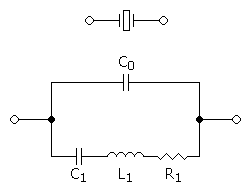
The shunt capacitance, C0, is the capacitance of the crystal's leads and package and is the only real value in the equivalent circuit. C1 is an equivalent value, a value that only exists in the model. Actual measurements for these values may or may not (and probably won't) be given in the crystal's datasheet. The crystal I'm using has a shunt capacitance C0 of 1.35pF typical, but the value C1 is not given. I was able to find one reference that gave typical values for C1 as 5-30fF (femtofarads). According to some resources I found, you might be able to pull a crystal by 100 or 200ppm. For the 32.768 kHz crystal I'm using, 100ppm would be 3.27Hz. In more realistic terms, 100ppm is about 8 seconds per day. Assuming I've chosen my load capacitors correctly, the +/- 20ppm rating of the crystal is about 1.8 seconds per day.
This is hardly a comprehensive review of the subject. I'm sure there's lots more to know about choosing capacitors that I either haven't found or don't care to dig in to. I'm hoping this information is enough to let me choose suitable capacitors for my designs, and I hope it is for you, too. But I have to say this again: just because I write a blog doesn't make me an expert.
Additional References:
http://www.crystek.com/documents/appnotes/PierceGateLoadCap.pdf
http://en.wikipedia.org/wiki/Pierce_oscillator
http://www.fairchildsemi.com/an/AN/AN-340.pdf
http://www.crystek.com/documents/appnotes/Pierce-GateIntroduction.pdf
http://www.freescale.com/files/microcontrollers/doc/app_note/AN3208.pdf
http://www.atmel.com/Images/doc8128.pdf


Hi Matthew,
This is the simplest and most explaining article I ve found on the internet so far. So thank you.
The bias resistor between the inverter’s input and output, forces the inverter into its linear mode (input & output at Vcc / 2), essentially turning it into an amplifier with a ballpark gain of 20 (varies).
This is a very unstable state for the inverter, as a small signal at its input will make the inverter want to change its output.
Since the inverter’s output signal is fed back into its input, with a small built-in delay inherent to the inverter’s design (also affected by Vcc and temperature), the inverter’s output will oscillate. No additional parts required!
Great, so now we have uncontrolled oscillations! Now to remove the frequencies we don’t want, or at least reduce their amplitude so they are not the dominant frequency on the output.
The goal is to build a filter network that has a gain of 1 at the desired frequency, ie. so that gain = losses and oscillations will be sustained. There are many ways to do this, and using a crystal makes for a very selective filter network (high quality, or high Q).
If the output gain is lower than 1, then the oscillations will decay in amplitude, and eventually stop oscillating. Good for unwanted frequencies, bad for the desired frequency… we need a band-pass filter network!
If the output gain is higher than 1, then the oscillations will grow resulting in a distorted clipped waveform, at possibly the wrong (or constantly changing) frequency, and possibly damaging the crystal from too much applied power. Bad for all frequencies! Hence a series resistor is sometimes required to limit inverter output gain, especially a large resistance value (example: 220 kOhms) with very low-power 32.768 kHz “tuning fork” crystals.
But, how do we control gain?
Well, you don’t need to control it per se, but you do need to limit it, thanks to the inverter being better at amplifying low frequencies than amplifying high frequencies. If you made a graph of gain vs. frequency, gain would appear to decrease with increasing frequency (looks like a hill, with a frequency beyond which the gain rapidly drops, or “rolls-off). However, this decreasing gain can cause a problem when the desired frequency is higher, i.e. not enough gain = oscillations decay in amplitude below the sustaining 1 gain.
Sine waves in phase reinforce (1 + 1 = 2). Sine waves 180 degrees out of phase cancel (1 + -1 = 0). We can use a difference of phase shift to build a filter!
The crystal and capacitors form a PI band-pass filter. [Queue the trumpets: “Ta-Da!”]
Each element provides roughly 90 degrees of phase shift to the input signal at the desired frequency, so the output signal is 180 degrees out of phase with the input signal, or inverted … wait … the inverter also adds 180 degrees of phase shift! That’s 360 degrees of phase shift total!
The inverter’s output signal is in phase with the input signal to the PI network, reinforcing the signal entering the PI network = sustained oscillation if the gain is sufficient.
To complicate matters slightly, the inverter actually adds slightly more then 180 degrees of phase shift, since it has built-in gate delay that varies with frequency, remember? This can be compensated with small changes to the capacitors, especially the one on the input of the network.
Reducing gain is easy, but what if I need a bit more gain in my oscillator?
Well, the capacitors basically exchange charge, so if the input capacitor is slightly larger than the output capacitor, crystal losses can be compensated. This also makes the circuit more likely to oscillate (more gain) at low frequencies (during start-up). Of course it takes more time (lower frequency response), and power, to charge a larger capacitor. It’s a trade-off.
Good explanation. 🙂
Answered all my questions on the subject. Keep it up!
Thanks you for this explanation, straight forward and answer all my doubts.
Best explanation I’ve seen.
Just came across your site. Great info here. Also was difficult to find for me as well. I see this is from 2014. Are you still posting?
Hey thanks for putting that all together, very useful! Surprisingly hard to get this straightforward info.
Thanks for your post!
I thought about that thing, why these capacitors are always put to gnd not just parallel to the crystal.
I think it has to do with the caps not having any reference voltage this way, since one end basicly is tied to a high impedance input of the inverter, which is the same as if it were hanging in the air (although this input of course measures the voltage). But you couldn’t charge/discharge a cap without it somehow having a defined gnd connection.
What do you think of that?
Thanks for your post,
Johannes
Thanks for your post
Good explanation and it clarifies all my doubts
Very useful
Keep give this kind of information for all of us
I just made a simple calculator: https://www.afdhalatifftan.com/2019/06/crystal-capacitor-calculator.html
What type of capacitor for microcontroller oscillators? Silver mica, ceramic, (metal) film? Does it matter (excluding electrolytics)?